
Every Nanometer Counts, and So Does Every Megahertz
Qualcomm just told us the headline clock speed for its next flagship CPU before it has even named the chip. The Oryon core inside the presumed Snapdragon 8 Elite Gen 6 will hit up to 5GHz, according to an OnQ blog post published ahead of Snapdragon Summit 2026 in Maui on September 22-24. That makes it the first mobile CPU core to clear the 5GHz wall, a threshold that took desktop silicon over a decade to approach comfortably and that phone SoCs have been creeping toward for the last three generations.
Context matters here. The 8 Elite Gen 5 topped out at 4.74 GHz. The chip before that landed at 4.47 GHz. That is roughly a 260 MHz jump generation over generation for most of Qualcomm's Oryon era, so a leap to 5.0 GHz is a bigger step than the recent trend line suggested. Qualcomm is crediting a fully custom microarchitecture redesign, not just a node shrink, for getting there. That distinction matters because clock speed gains that come purely from moving to a denser TSMC process tend to buy you maybe 5-8% before leakage and thermal density fight back. A structural redesign of the pipeline, the clock distribution network, and the physical implementation is what lets you push past that ceiling without melting a phone chassis.
The Real Story Isn't the Clock, It's FlexCache
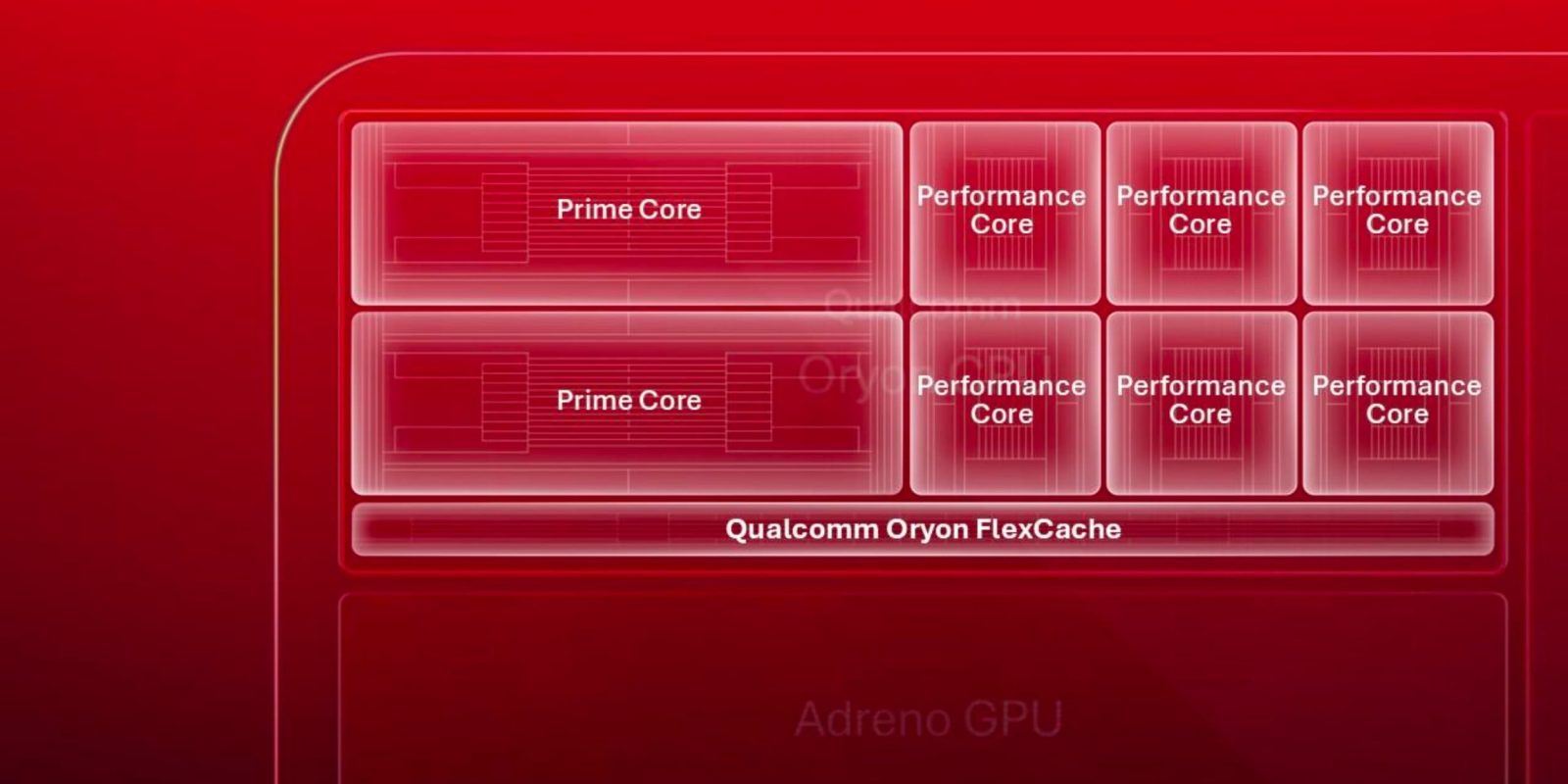
Any chip architect will tell you clock speed is the easy number to market and the hard number to sustain. The more interesting disclosure buried in the same post is FlexCache, Qualcomm's new shared L2 cache architecture. Every mobile SoC to date, Oryon included, has partitioned L2 cache rigidly: each core gets its own fixed slice, and if one core needs more working set than its slice allows, data spills out to system memory or a shared L3, both of which cost latency and power.
FlexCache pools L2 across the CPU cluster into a single addressable space that any core, prime or performance, can draw from dynamically. When a Prime core is running a latency-sensitive single-thread workload, like the UI thread during a big game load or a camera capture pipeline, it can borrow cache capacity that idle Performance cores aren't using. When the workload shifts to multi-threaded background sync, the allocation shifts with it. This is conceptually similar to what AMD does with 3D V-Cache sharing across a CCD, except Qualcomm is doing it across a heterogeneous 2P+6P cluster with wildly different core types and power budgets, which is a harder cache-coherency problem than mirroring identical cores.
Why Heterogeneous Cache Sharing Is Genuinely Hard
On a desktop CCD, every core is architecturally identical, so a shared cache slice behaves predictably no matter which core touches it. Oryon's cluster mixes Prime cores tuned for peak single-thread performance with Performance cores tuned for sustained efficiency, and those cores likely have different cache access latencies and coherency traffic patterns even when they're pulling from the same physical SRAM pool. Getting a shared cache to serve both without introducing snoop overhead that eats the very latency gains you're chasing is a nontrivial implementation problem. Qualcomm's claim that Prime cores can access the entire pool when needed, rather than a negotiated subset, suggests they've built a fairly aggressive arbitration scheme, and arbitration schemes are usually where shared-cache designs either shine or fall apart under real workloads.
What This Means for the Actual Chip War
Qualcomm has not confirmed the final name, node, or transistor count for this silicon, and no GPU or NPU details have been shared yet. Those will reportedly trickle out in the weeks before the Summit. But the sequencing itself is a tell: leading with CPU microarchitecture rather than AI TOPS numbers is a shift in how Qualcomm wants this generation perceived, especially with Apple's A-series and MediaTek's Dimensity flagships both closing the single-thread gap that used to be Qualcomm's clearest advantage.
A 5GHz peak clock on a phone SoC will not sustain indefinitely under thermal load, and burst clocks on mobile silicon are notoriously short-lived once a chassis heats up. The number that will actually matter come launch day is sustained clock under a 10-minute gaming loop, not the marketing peak. Still, a genuine microarchitecture overhaul paired with a smarter cache hierarchy is a more credible efficiency story than another marginal clock bump, and it's the kind of low-level engineering change that tends to pay dividends across two or three product generations rather than one flashy keynote slide.
Loading comments...